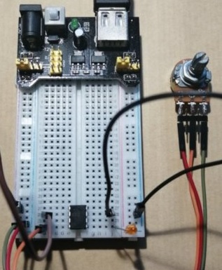
PIC で RS232c通信を行う で作ったシリアル通信の仕組みで、
パソコンに変換データを送りたいと思います。#include <stdio.h>
#include <stdlib.h>
// CONFIG1
#pragma config FOSC = INTOSC // Oscillator Selection (INTOSC oscillator: I/O function on CLKIN pin)
#pragma config WDTE = OFF // Watchdog Timer Enable (WDT disabled)
#pragma config PWRTE = ON // Power-up Timer Enable (PWRT enabled)
#pragma config MCLRE = OFF // MCLR Pin Function Select (MCLR/VPP pin function is digital input)
#pragma config CP = OFF // Flash Program Memory Code Protection (Program memory code protection is disabled)
#pragma config CPD = OFF // Data Memory Code Protection (Data memory code protection is disabled)
#pragma config BOREN = ON // Brown-out Reset Enable (Brown-out Reset enabled)
#pragma config CLKOUTEN = OFF // Clock Out Enable (CLKOUT function is disabled. I/O or oscillator function on the CLKOUT pin)
#pragma config IESO = OFF // Internal/External Switchover (Internal/External Switchover mode is disabled)
#pragma config FCMEN = OFF // Fail-Safe Clock Monitor Enable (Fail-Safe Clock Monitor is disabled)
// CONFIG2
#pragma config WRT = OFF // Flash Memory Self-Write Protection (Write protection off)
#pragma config PLLEN = OFF // PLL Enable (4x PLL disabled)
#pragma config STVREN = ON // Stack Overflow/Underflow Reset Enable (Stack Overflow or Underflow will cause a Reset)
#pragma config BORV = HI // Brown-out Reset Voltage Selection (Brown-out Reset Voltage (Vbor), high trip point selected.)
#pragma config LVP = OFF // Low-Voltage Programming Enable (High-voltage on MCLR/VPP must be used for programming)
#include <xc.h>
#define _XTAL_FREQ 16000000
void send(unsigned char c) {
while (!TXIF);
TXREG = c;
}
void putch(char c) {
send(c);
}
int receive(unsigned char*c) {
if (RCIF) {
*c = RCREG;
return 0;
}
return -1;
}
void main() {
OSCCON = 0b01111010; //クロック周波数16MHz
ANSELA = 0b00000000; //ポートAをデジタル入力にする
ANSELB = 0b00000000; // ポートBをデジタル入力にする
PORTA = 0b00000000;
PORTB = 0b00000000;
TRISA = 0b00000000;
TRISB = 0b00000010; //RB1は入力にしないと受信できない
TXCKSEL = 0; // TX:RB2
RXDTSEL = 0; // RX:RB1
TXSTA = 0b00100100;
BRG16 = 1;
RCSTA = 0b10010000;
//ボーレート= FOSC /(4([SPBRGHx:SPBRGx] + 1))
// SPBRGHx:SPBRGx:=((FOSC / ボーレート)/ 4)-1
const uint16_t DBR = ((uint32_t) ((uint32_t) _XTAL_FREQ / 9600) / 4) - 1;
SPBRGH = (uint8_t) (DBR >> 8);
SPBRGL = (uint8_t) (DBR);
TRISA = 0b00000001; // RA0を入力にする
ANSELA = 0b00000001; // ポートAをデジタル入力、RA0をアナログ入力
WPUA = 0b11111110; // RA0の弱プルアップを無効
nWPUEN = 0; // WPUx ラッチの値に応じて弱プルアップを有効にする
//ADCON1 = 0b11100000; // 変換結果右詰め FOSC/64 VREF+をAVDD
ADCON1 = 0b11100011; // 変換結果右詰め FOSC/64 VREF+をFVR
FVRCON = 0b10000011; // FVR有効 出力4倍 (4.096 V)
while(!FVRRDY); // FVRが安定するまで待つ
ADCON0 = 0b00000001; // アナログチャンネルAN0 ADC有効
while (1) {
GO = 1; // 変換の開始
while (GO); // 変換の完了
printf("%d\r\n", ADRES); // 変換結果を出力
}
}
PIC で RS232c通信を行う で作成したプログラムです。
    ADCON1 = 0b11100000; // 変換結果右詰め FOSC/64 VREF+をAVDD
  //ADCON1 = 0b11100011; // 変換結果右詰め FOSC/64 VREF+をFVR
  //FVRCON = 0b10000011; // FVR有効 出力4倍 (4.096 V)
  //while(!FVRRDY);      // FVRが安定するまで待つ
ADCON0 = 0b00000001; // アナログチャンネルAN0 ADC有効 TRISA = 0b00010000; //RA4を入力にする
ANSELA = 0b00010000; //ポートAをデジタル入力、RA4をアナログ入力
WPUA = 0b11101111; //RA4の弱プルアップを無効
nWPUEN = 0; //WPUx ラッチの値に応じて弱プルアップを有効にする
//ADCON1 = 0b11100000; // 変換結果右詰め FOSC/64 VREF+をAVDD
ADCON1 = 0b11100011; // 変換結果右詰め FOSC/64 VREF+をFVR
FVRCON = 0b10000011; // FVR有効 出力4倍 (4.096 V)
while(!FVRRDY); //FVRが安定するまで待つ
ADCON0 = 0b00010001; // アナログチャンネルAN4 ADC有効
while (1) {
GO = 1; // 変換の開始
while (GO); // 変換の完了
printf("%d\r\n", ADRES); // 変換結果を出力
}
    TRISB =  0b00010000; // RB4は入力にする
    ANSELB = 0b00010000; // ポートBをデジタル入力、RB4をアナログ入力
    WPUB =   0b11101111; // RB4の弱プルアップを無効
    nWPUEN = 0;          // WPUx ラッチの値に応じて弱プルアップを有効にする

  //ADCON1 = 0b11100000; // 変換結果右詰め FOSC/64 VREF+をAVDD
    ADCON1 = 0b11100011; // 変換結果右詰め FOSC/64 VREF+をFVR
    FVRCON = 0b10000011; // FVR有効 出力4倍 (4.096 V)
    while(!FVRRDY);      // FVRが安定するまで待つ
    ADCON0 = 0b00100001; // アナログチャンネルAN8 ADC有効
#include <stdio.h>
#include <stdlib.h>
// CONFIG1
#pragma config FOSC = INTOSC    // Oscillator Selection (INTOSC oscillator: I/O function on CLKIN pin)
#pragma config WDTE = OFF       // Watchdog Timer Enable (WDT disabled)
#pragma config PWRTE = ON       // Power-up Timer Enable (PWRT enabled)
#pragma config MCLRE = OFF      // MCLR Pin Function Select (MCLR/VPP pin function is digital input)
#pragma config CP = OFF         // Flash Program Memory Code Protection (Program memory code protection is disabled)
#pragma config CPD = OFF        // Data Memory Code Protection (Data memory code protection is disabled)
#pragma config BOREN = ON       // Brown-out Reset Enable (Brown-out Reset enabled)
#pragma config CLKOUTEN = OFF   // Clock Out Enable (CLKOUT function is disabled. I/O or oscillator function on the CLKOUT pin)
#pragma config IESO = OFF       // Internal/External Switchover (Internal/External Switchover mode is disabled)
#pragma config FCMEN = OFF      // Fail-Safe Clock Monitor Enable (Fail-Safe Clock Monitor is disabled)
// CONFIG2
#pragma config WRT = OFF        // Flash Memory Self-Write Protection (Write protection off)
#pragma config PLLEN = OFF      // PLL Enable (4x PLL disabled)
#pragma config STVREN = ON      // Stack Overflow/Underflow Reset Enable (Stack Overflow or Underflow will cause a Reset)
#pragma config BORV = HI        // Brown-out Reset Voltage Selection (Brown-out Reset Voltage (Vbor), high trip point selected.)
#pragma config LVP = OFF        // Low-Voltage Programming Enable (High-voltage on MCLR/VPP must be used for programming)

#include <xc.h>
#define _XTAL_FREQ 16000000

void send(unsigned char c) {
    while (!TXIF);
    TXREG = c;
}

//数字を送信する
void print(unsigned int n) {
    unsigned int p = 10000;
    unsigned char i;
    while (p) {
        i = 0;
        while (n >= p) {
            i++;
            n = n - p;
        }
        send('0' + i);
        p = p / 10;
    }
    send('\r');
    send('\n');
}

int receive(unsigned char*c) {
    if (RCIF) {
        *c = RCREG;
        return 0;
    }
    return -1;
}

void main() {
    OSCCON = 0b01111010; // クロック周波数16MHz
    ANSELA = 0b00000100; // ポートAをデジタル入力にする RA2はアナログ入力
    PORTA = 0b00000000;
    TRISA = 0b00000110; // RA1は入力にしないと受信できない RA2は入力にする
    WPUA = 0b11111011; // RA2の弱プルアップを無効
    nWPUEN = 0; // WPUx ラッチの値に応じて弱プルアップを有効にする

    TXCKSEL = 0; // TX:RA0
    RXDTSEL = 0; // RX:RA1

    TXSTA = 0b00100100;
    BRG16 = 1;
    RCSTA = 0b10010000;

    //ボーレート= FOSC /(4([SPBRGHx:SPBRGx] + 1))
    // SPBRGHx:SPBRGx:=((FOSC / ボーレート)/ 4)-1

    const uint16_t DBR = ((uint32_t) ((uint32_t) _XTAL_FREQ / 9600) / 4) - 1;

    SPBRGH = (uint8_t) (DBR >> 8);
    SPBRGL = (uint8_t) (DBR);

    //ADCON1 = 0b11100000; // 変換結果右詰め FOSC/64 VREF+をAVDD
    ADCON1 = 0b11100011; // 変換結果右詰め FOSC/64 VREF+をFVR
    FVRCON = 0b10000011; // FVR有効 出力4倍 (4.096 V)
    while (!FVRRDY); // FVRが安定するまで待つ
    ADCON0 = 0b00001001; // アナログチャンネルAN2 ADC有効

    while (1) {
        GO = 1; // 変換の開始
        while (GO); // 変換の完了
        // printf("%d\r\n", ADRES); // 変換結果を出力 メモリーが足りなくなるため使用できない
        print(ADRES);//数字をシリアル通信で送信する
    }
}
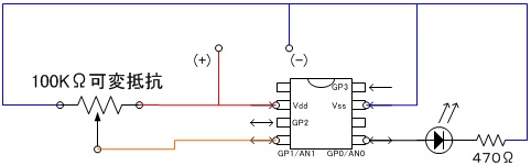
printf("%d\r\n", ADRES); とすると、この行一つでメモリーが足りなくなります。#include <stdio.h>
#include <stdlib.h>
#pragma config IOSCFS = 8MHZ // Internal Oscillator Frequency Select bit (8 MHz)
#pragma config MCPU = OFF // Master Clear Pull-up Enable bit (Pull-up enabled)
#pragma config WDTE = OFF // Watchdog Timer Enable bit (WDT disabled)
#pragma config CP = OFF // Code protection bit (Code protection off)
#pragma config MCLRE = OFF // GP3/MCLR Pin Function Select bit (GP3/MCLR pin function is digital I/O, MCLR internally tied to VDD)
#include <xc.h>
#define _XTAL_FREQ 8000000 //クロック周波数 __delay_ms()に必要
int main(int argc, char** argv) {
OSCCAL = 0b00000000;
OPTION = 0B11000000;
ADCON0 = 0B00100101;
TRISGPIO = 0b00000010;
int i;
while (1) {
GO = 1; // 変換の開始
while (GO); // 変換の完了
GPIO = 0b00000000; //GPIOに出力
for (i = 0; i < ADRES; i++) __delay_ms(1);
GPIO = 0b00000111;
for (i = 0; i < ADRES; i++) __delay_ms(1);
}
return (EXIT_SUCCESS);
}
ADCON0 の設定部分、英語版データシートを開くと次のように書いてあります。
bit 7 ANS1: ADC Analog Input Pin Select bit ▲トップページ
>
マイコンなど